Novel submicron infrared microspectroscopy for failure analysis of semiconductor devices
Sub-micron IR spatial resolution – 30x better than traditional FTIR/QCL microscopy
Non-contact, non-destructive, reflection mode measurements with FTIR transmission/ATR-like spectral quality directly library searchable
O-PTIR provides superior measurement of dark colored, light sensitive samples currently limited by existing Raman microscopy
Simultaneous O-PTIR and Raman for complimentary and confirmatory analysis with faster time to data and enhanced data confidence
Unique co-located fluorescence microscopy for faster localization of organic contaminants, for subsequent O-PTIR analysis
Download application notes here:
Failure analysis of semiconductor devices
PDF: Novel sub-micron infrared microspectroscopy for failure analysis of semiconductor devices
PDF: Sub-micron IR for failure analysis in semiconductor and microelectronics
Sub-micron organic contamination in hard drives
PDF: Sub-micron IR spectroscopy of defects in semiconductor packaging recessed structures
Sub-micron IR resolution chemical imaging of failed device features
High resolution chemical imaging of failed device features
Figure opposite illustrates how O-PTIR overcomes existing challenges of infrared spectroscopy techniques with an example highlighting the dark suspected creep in the underfill (UF) between two metal cross-sectioned surfaces [Zulkifli, 2022]. With the O-PTIR technique, several components can be spectroscopically separated and identified. Here, the top 3µm of the dark contamination has been identified as an epoxy component, which is usually the organic binder component in underfill materials.
The bottom 3µm layer appears to contain significant amounts of carbon and carboxylates; the latter may have originated from oxidized cellulosic matter. Such unprecedented details provide investigative insights into tracking down the source of the contamination, raw materials, or errors in the process. In contrast, conventional FT-IR microspectroscopy could not provide

Sub-micron O-PTIR spectroscopy and imaging analysis of a suspected creep specimen.
meaningful information from the same specimen [Zulkifli, 2022].
Finally, the analysis was achieved from a cross-sectioned surface using standard chemo-mechanically polishing processes, representing a significant time savings over more involved sample preparation techniques, such as those requiring labor-intensive focused ion beam (FIB)-based thin sectioning.
Overview of additional examples of sub-micron IR failure analysis applications

Left; visible image showing location of 6µm defect, Upper Right; Comparison of unknown O-PTIR spectrum to nearest library match, Lower Right: Comparison of unknown Raman spectrum to nearest library match

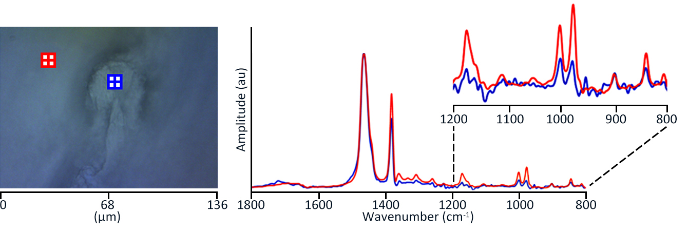
Upper Left; Schematic representation of sample and measurement, Lower Left; Visible camera image of defect, Right; O-PTIR spectra from on and off the defect. Colors correspond to markers on visible image
Left: Optical image of defect in a 240 µm thick two layer film. Markers on image represent the location of subsequent O-PTIR spectral collection. Right: Spectra collected in the defect-free (red) and defect (blue) region of the sample. The spectra display peaks indicative of isotactic polypropylene (998 cm-1). Insert: In the plot of the varying intensities for the isotactic polypropylene peak, both on the defect and off, The film region shows consistent signal intensity, while the defect region shows significant variability.
Simultaneous IR+Raman spectral searching with 2D search result representation with KnowItAll®
One of the goals of any FA process is the chemical identification of the unknown material and to that end, the final step, after spectral acquisition is to search against a spectral database. Traditionally IR spectra would be searched against an IR spectral library and Raman spectral would be searched, separately, against a Raman spectral library. The user would then examine the two separate so-called “hitlists” for IR and Raman spectra.
Now, with the advent of simultaneous submicron IR+Raman spectral acquisition, as seen in figure here, not only are the IR and Raman spectra simultaneously collected, but now the spectral search of both IR and Raman spectral occur simultaneously, with a single click from the data acquisition software.
Furthermore, to aid in evaluating the results, the IR and Raman hit lists are

presented in a 2D scatter plot, with the IR Hit Quality Index (HQI) plotted on one axis and the Raman HQI plotted on the other axis as shown in the figure above.
For more information on Wiley’s KnowItAll® products, click here
Download the product flyer here:
Wiley KnowItAll®
Solutions to accelerate IR and Raman analysis

Novel submicron infrared microspectroscopy for failure analysis of semiconductor devices
Sub-micron IR spatial resolution – 30x better than traditional FTIR/QCL microscopy
Non-contact, non-destructive, reflection mode measurements with FTIR transmission/ATR-like spectral quality directly library searchable
O-PTIR provides superior measurement of dark colored, light sensitive samples currently limited by existing Raman microscopy
Simultaneous O-PTIR and Raman for complimentary and confirmatory analysis with faster time to data and enhanced data confidence
Unique co-located fluorescence microscopy for faster localization of organic contaminants, for subsequent O-PTIR analysis
Download application notes here:
Failure analysis of semiconductor devices
PDF: Novel sub-micron infrared microspectroscopy for failure analysis of semiconductor devices
PDF: Sub-micron IR for failure analysis in semiconductor and microelectronics
Sub-micron organic contamination in hard drives
PDF: Sub-micron IR spectroscopy of defects in semiconductor packaging recessed structures
Sub-micron IR resolution chemical imaging of failed device features
High resolution chemical imaging of failed device features
Figure opposite illustrates how O-PTIR overcomes existing challenges of infrared spectroscopy techniques with an example highlighting the dark suspected creep in the underfill (UF) between two metal cross-sectioned surfaces [Zulkifli, 2022]. With the O-PTIR technique, several components can be spectroscopically separated and identified. Here, the top 3µm of the dark contamination has been identified as an epoxy component, which is usually the organic binder component in underfill materials.
The bottom 3µm layer appears to contain significant amounts of carbon and carboxylates; the latter may have originated from oxidized cellulosic matter. Such unprecedented details provide investigative insights into tracking down the source of the contamination, raw materials, or errors in the process. In contrast, conventional FT-IR microspectroscopy could not provide
Sub-micron O-PTIR spectroscopy and imaging analysis of a suspected creep specimen.
meaningful information from the same specimen [Zulkifli, 2022].
Finally, the analysis was achieved from a cross-sectioned surface using standard chemo-mechanically polishing processes, representing a significant time savings over more involved sample preparation techniques, such as those requiring labor-intensive focused ion beam (FIB)-based thin sectioning.
Overview of additional examples of sub-micron IR failure analysis applications
Left; visible image showing location of 6µm defect, Upper Right; Comparison of unknown O-PTIR spectrum to nearest library match, Lower Right: Comparison of unknown Raman spectrum to nearest library match
Upper Left; Schematic representation of sample and measurement, Lower Left; Visible camera image of defect, Right; O-PTIR spectra from on and off the defect. Colors correspond to markers on visible image
Left: Optical image of defect in a 240 µm thick two layer film. Markers on image represent the location of subsequent O-PTIR spectral collection. Right: Spectra collected in the defect-free (red) and defect (blue) region of the sample. The spectra display peaks indicative of isotactic polypropylene (998 cm-1). Insert: In the plot of the varying intensities for the isotactic polypropylene peak, both on the defect and off, The film region shows consistent signal intensity, while the defect region shows significant variability.
Simultaneous IR+Raman spectral searching with 2D search result representation with KnowItAll®
Now, with the advent of simultaneous submicron IR+Raman spectral acquisition, as seen in figure here, not only are the IR and Raman spectra simultaneously collected, but now the spectral search of both IR and Raman spectral occur simultaneously, with a single click from the data acquisition software.
Furthermore, to aid in evaluating the results, the IR and Raman hit lists are presented in a 2D scatter plot, with the IR Hit Quality Index (HQI) plotted on one axis and the Raman HQI plotted on the other axis as shown in the figure above.
For more information on Wiley’s KnowItAll® products, click here
Download the product flyer here:
Wiley KnowItAll®
Solutions to accelerate IR and Raman analysis

Photothermal Spectroscopy Corp.
325 Chapala Street
Santa Barbara, CA 93101
Phone: (805) 845-6568
Email: info [at] photothermal.com