
Application note
Novel sub-micron infrared microspectroscopy for failure analysis of semiconductor devices

O-PTIR spectroscopy offers unique capabilities for failure analysis applications:
- Submicron IR spatial resolution, 30x better than traditional FTIR/QCL microscopy
- Non-contact, non-destructive, reflection (far-field) mode measurements with little to no sample preparation
- High quality spectra (particle shape/size and surface roughness independent) with no dispersive/scatter artefacts that are directly searchable in commercial/custom FTIR transmission or ATR libraries
- Simultaneous O-PTIR and Raman measurement of devices for complementary and confirmatory results with faster time to data and enhanced data confidence
- O-PTIR provides superior measurement of high resolution, dark colored, light sensitive samples currently limited by existing Raman and FTIR techniques
- Offers unique co-located fluorescence microscopy for fast identification of organic contaminants and faster time to data
What is O-PTIR
The O-PTIR technique overcomes the IR diffraction limit associated with traditional IR microscopy techniques by illuminating the sample with a mid-IR pulsed tunable quantum cascade laser (QCL) and measuring infrared absorption, indirectly with a visible laser beam.
When the QCL laser is tuned to a wavelength that excites molecular vibrations in the sample, absorption occurs, thereby creating photothermal effects, e.g., sample surface expansion and a change in refractive index.
Advances in semiconductor technology have fueled growth in a wide range of areas in everyday life with ongoing developments of cutting-edge phones, computers, automobiles, information technology development, artificial intelligence, and have also significantly contributed to the improved quality of life for populations around the world.
These advances continue to drive increased investment into the technology and manufacture of semiconductor devices at both industrial and academic research levels. Technology improvements such as increasingly narrow semiconductor linewidths, new materials, manufacturing processes and device structures are all driving requirements for new metrology and inspection techniques for both in-line, off-line and failure analysis.
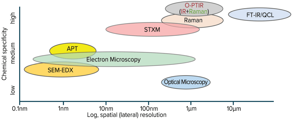
The Failure Analysis (FA) process and technologies help manufacturers to determine the cause of failure in a semiconductor device. The analysis involves a wide range of processes and measurement equipment to determine the root cause with the goal of avoiding a reoccurrence in the future. FA measurement techniques vary in terms of chemical specificity, spatial resolution, sample preparation requirements, data acquisition and analysis time, complexity, automation capabilities, and cost.
For example, Scanning Electron Microcopy when coupled with Energy Dispersive X-Ray (SEM-EDX) Spectroscopy, can provide excellent spatial resolution, but with only elemental chemical information as seen in figure 1. Often, elemental information alone is not sufficient to provide a high confidence unknown identification and organic molecular information is required to identify unknowns with a high degree of confidence. Technologies like Infrared (IR) and Raman microspectroscopy are common and well-established techniques in FA that provide organic molecular information.
For chemical imaging, Raman and FT-IR spectroscopy equipment provide broad, spatially resolved chemical characterization capabilities that have been applied to a wide range of application areas: foreign materials analysis, device degradation, raw material impurity qualification, formulation errors; all of which could lead to early failure of components and devices within semiconductor and electronic products.
However, conventional FT-IR microscopy is limited in its spatial resolution and sensitivity for FA, while Raman microscopy often has low sensitivity for many samples due to autofluorescence issues and can lead to laser-induced sample damage, especially with darker materials. A new technique, Optical Photothermal Infrared (O-PTIR) microscopy, can overcome many of abovementioned limitations, while maintaining the complementary nature of Raman and IR. O-PTIR also has seamless integration with both Raman spectroscopy and fluorescence microscopy to locate specific organic contaminants to help guide the subsequent IR measurement. Figure 1 provides a graphical representation of a range of typical analytical techniques in FA, plotted against spatial resolution and chemical information content.
This application note describes the novel O-PTIR approach and its integration with Raman and fluorescence techniques for failure analysis applications on the mIRage-LS platform. We will also discuss a wide range of high value application failure analysis examples.
Optical Photothermal IR (O-PTIR) spectroscopy with simultaneous Raman spectroscopy
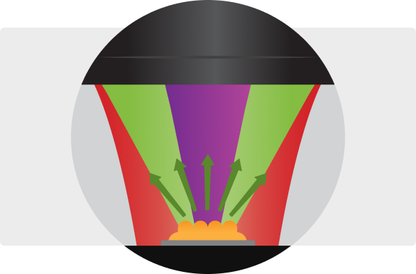
The O-PTIR technique overcomes the IR diffraction limit associated with traditional IR microscopy techniques by illuminating the sample with a mid-IR pulsed tunable quantum cascade laser (QCL) and measuring infrared absorption, indirectly with a visible laser beam (532nm). When the QCL laser is tuned to a wavelength that excites molecular vibrations in the sample, absorption occurs, thereby creating photothermal effects, e.g. sample surface expansion and a change in refractive index. The visible probe laser, focused to sub-micron spot size, measures this photothermal response via a modulation induced in the scattered light, as shown in figure 2. The IR laser can be swept through the entire range in under two seconds to obtain an IR spectrum.
Furthermore, the visible probe laser also generates Raman scattered light from the same measurement area, which when collected, allows for the simultaneous acquisition of both IR and Raman spectra, with the same submicron spatial resolution, at the same location and at the same time. A schematic diagram for this optical beam path is shown below in figure 3. With this simultaneous measurement capability, researchers can utilize the complementary nature of both techniques and provide confirmatory spectral information for more accurate measurements.
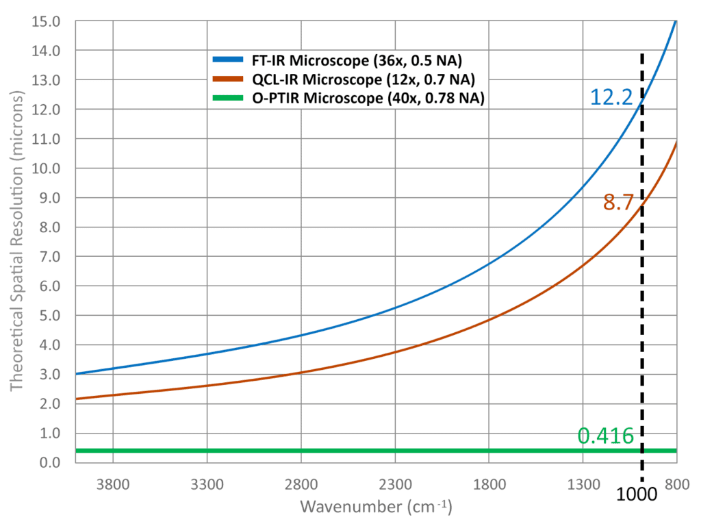
Figure 4 illustrates the variable spatial resolutions in common IR microscope systems over the traditional infrared range using two IR objectives of 0.5 or 0.7NA versus the constant spatial resolution of the O-PTIR technique using a 0.78NA objective (Kansiz, 2020). The O-PTIR technique provides wavenumber independent spatial resolution over the entire mid-IR range due to the use of a fixed wavelength probe beam at 532nm.

mIRage-LS principal of operation: O-PTIR and fluorescence microscopy
The system layout for a combined O-PTIR sub-micrometer IR microscope, co-located with fluorescence microscopy is illustrated in figure 5. In counter propagating mode, the pulsed IR beam is directed through the underside of the sample. The fluorescence and visible probe beam paths are co-located through the microscope objective.

Simultaneous IR+Raman spectral searching with 2D search result representation with KnowItAll®
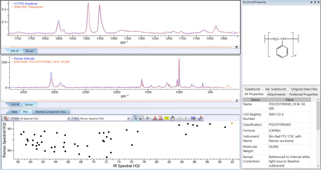
One of the goals of any FA process is the chemical identification of the unknown material and to that end, the final step, after spectral acquisition is to search against a spectral database. Traditionally IR spectra would be searched against an IR spectral library and Raman spectral would be searched, separately, against a Raman spectral library. The user would then examine the two separate so-called “hitlists” for IR and Raman spectra. Now, with the advent of simultaneous submicron IR+Raman spectral acquisition, as seen in figure 6, not only are the IR and Raman spectra simultaneously collected, but now the spectral search of both IR and Raman spectral occur simultaneously, with a single click from the data acquisition software. Furthermore, to aid in evaluating the results, the IR and Raman hit lists are presented in a 2D scatter plot, with the IR Hit Quality Index (HQI) plotted on one axis and the Raman HQI plotted on the other axis. Figure 6 provides an example of a simultaneous IR+Raman search result for a common plastic. In such a 2D scatterplot, the best result is to be found in the upper right corner of the plot, where
the result indicates a both a high IR and high Raman HQI, thus providing for that confirmatory aspect as well as being complementary.
The benefits of this unique approach are two-fold;
- Productivity and ease-of-use gains, through the simple one-button spectral export and loading into KnowItAll® presenting the data to the analyst ready to be searched and answers delivered.
- The increased accuracy and confidence in your data that comes with IR+Raman spectral providing both complementary and confirmatory data, i.e. IR search result can confirm the Raman and vice-versa.
High value failure analysis applications with O-PTIR and combined techniques
High resolution chemical imaging of failed device features
Figure 7 illustrates how O-PTIR overcomes existing challenges of infrared spectroscopy techniques with an example highlighting the dark suspected creep in the underfill (UF) between two metal cross-sectioned surfaces (Zulkifli, 2022). With the O-PTIR technique, several components can be spectroscopically separated and identified. Here, the top 3µm of the dark contamination has been identified as an epoxy component, which is usually the organic binder component in underfill materials.
The bottom 3µm layer appears to contain significant amounts of carbon and carboxylates; the latter may have originated from oxidized cellulosic matter [Madorsky, 1958]. Such unprecedented details provide investigative insights into tracking down the source of the contamination, raw materials, or errors in the process. In contrast, conventional FT-IR microspectroscopy could not provide meaningful information from the same specimen (Zulkifli, 2022).
A key advantage of using O-PTIR for this measurement is that the sample preparation used standard chemo-mechanical polishing techniques representing a significant time saving over more involved techniques, such as labor intensive focused ion beam sectioning.

Failure analysis of a capacitor devices with simultaneous O-PTIR and Raman
Polished cross-sections of capacitors with dark organic-metal multilayer structures are classic examples of a sample type that highlights the benefits of simultaneous O-PTIR and Raman analysis.
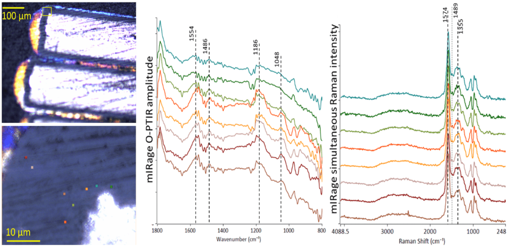
Figure 8 shows a typical cross-section of an electrolytic capacitor (E-cap): a thin, 10µm layer of dielectric material sandwiched between the metal casing and center electrode. The organic material absorbs infrared broadly and strongly, consistent with a dark-colored conductive polymer, thus, very little infrared light can reflect back to the infrared detector in an FT-IR measurement. Such an experiment typically results in poor, noisy FT-IR spectra with very few intelligible spectroscopic details (Zulkifli, 2022). Measuring the IR spectrum using an ATR accessory is problematic due to difficulty achieving good optical contact between the internal reflection element (IRE) and the hard metallic material which can also damage IRE.
The O-PTIR technique overcomes these challenges by collecting spectra from a submicrometer sample spot size in a non-contact reflection measurement. The result is transmission-like IR spectral band shapes, which originate from the smaller sampling area probed by the visible laser and localized sensing of photothermal effect.
In Figure 8, the strong O-PTIR baseline confirms the broad, strong IR absorption characteristics of the dark dielectric layer. O-PTIR spectra demonstrate spatially resolved spectroscopic differences, which have broadened IR absorption profiles caused by the presence of graphitic carbon. The dielectric’s chemistry is the most consistent with a polyphenylene derivative (Furukawa, 2002). The submicrometer O-PTIR and simultaneous Raman acquisition allow definitive characterization of both polar and non-polar species at the same spot at the same time. Here, the strong Raman shifts at 1574cm-1 and 1355cm-1 are consistent with graphite (Tunistra, 1970), thus confirming the observation in the corresponding O-PTIR spectra. In contrast, the cross-section of a cracked E-cap has a significantly different chemical signature than the normal specimen.
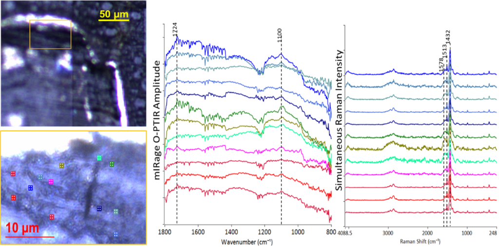
While strong spectral baseline offset is observed in Figure 9, O-PTIR spectral band shapes are vastly different and a new 1100cm-1 signal becomes apparent at many marker locations. The 1100cm-1 band is likely due to the presence of a polyethylene glycol derivative, which is a known reagent for improving the performance of electrolytic capacitors (Xiong, 2012). The simultaneous Raman feature of the instrument produces a sharp spectral signature consistent with PEDOT:PSS (Chang, 2014), which is likely the major component. The combined submicrometer O-PTIR and Raman simultaneous analysis provides a highly effective tool for accurately identifying unknown compositions that would have been challenging if not impossible, if conducted separately. The rough topography of the cross-section does not inhibit the identification process. These results from the combined approach have shown that the organic dielectric layer from the two suppliers are chemically different and that the composition of the cracked E-cap may have contributed to the failure.
O-PTIR for measurement of dark colored light sensitive materials
Identifying chemical compositions of foreign matter in an open circuit makes up one of most prevalent, long-standing industrial problems in microelectronics failure analysis. Unfortunately, the layers in these devices are often narrower than the diffraction limits of micrometer-sized infrared wavelengths, thus challenging the resolving power of conventional FT-IR microscopes. Raman microscopy could be a capable alternative spectroscopic technique to measure these samples, but the samples dark coloration often causes excessive heating and fluorescence, even leading to sample damage. Lowering the laser power to reduce heating results in Raman spectra with SNRs too low to provide adequate chemical information from the tested area and/or impractically long measurement times.
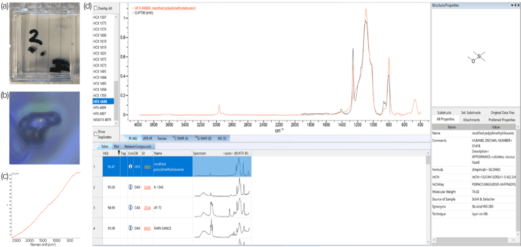
Since Raman scattering only occurs approximately once per one-million incident photons, high signal-to-noise measurements require strong sample illumination; unfortunately, that could lead to sample burning or melting. Figure 10 provides an example of samples that melt easily at standard Raman laser power levels, resulting in sample destruction (Anderson, 2022). A standard dark sample – fig.10(a) measured with Raman causes sample damage, figure 10(b) and poor quality Raman spectra 10(c). Even in cases with no sample damage at low milliwatt laser power levels, Raman spectra would have little value due to a strong auto-fluorescence baseline that can arise from illuminating strongly colored materials.
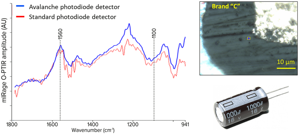
Collecting O-PTIR data with an avalanche photodiode (APD) detector enhances and overcomes inherently low sample reflectivity from dark colored and/or rough samples, while providing high spatial resolution. Figure 11 illustrates the high sensitivity of the APD at low probe laser illumination levels, that are well below the sample’s laser damage threshold. When compared with the standard detector, the use of APD yields higher SNR data, thus bringing greatly enhanced clarity and confidence to material differentiation. The rough topography of such samples does not prevent acquisition of high SNR infrared absorption spectrum with mIRage O-PTIR using an APD.
Fast identification of regions of interest using co-located fluorescence and O-PTIR
The O-PTIR technique has proven successful at determining the chemical identity of challenging samples, which has not been possible using the limited spatial resolution and sensitivity afforded by conventional infrared microspectroscopy. The non-contact operational nature of Raman microscopy is often limited by strong autofluorescence (AF) inherently present in many materials and poor spectral sensitivity. In a fast paced, high-throughput testing facility, quick and efficient data acquisition is of utmost importance. The brightfield or optical camera in the mIRage instrument produces a high quality visible image from which the user can easily and quickly highlight regions for subsequent OPTIR measurements. However, sometimes there is insufficient contrast in the visible image to alert or guide the user as to the whereabouts of the defects, known or unknown. As demonstrated in the previous examples, the spatial composition can be complex; it would be extremely helpful and timesaving to have localization and differentiation of species within of the region of interest (ROI) even before collecting the first O-PTIR (and simultaneous Raman) spectrum or image.
Fluorescence (FL) images can be obtained by exciting the region of interest (ROI) with different visible wavelengths and detecting the radiation re-emitted at longer wavelengths. Fluorescence imaging has been used for a long time in material science. The excitation and emission wavelengths of a given molecule are directly related to its inherent electronic states but would not affect O-PTIR data acquisition (Qin, 2020; Chen, 2022). As a result, widefield FL images can first map out the ROI before collecting the spatially resolved chemical information by submicron O-PTIR.
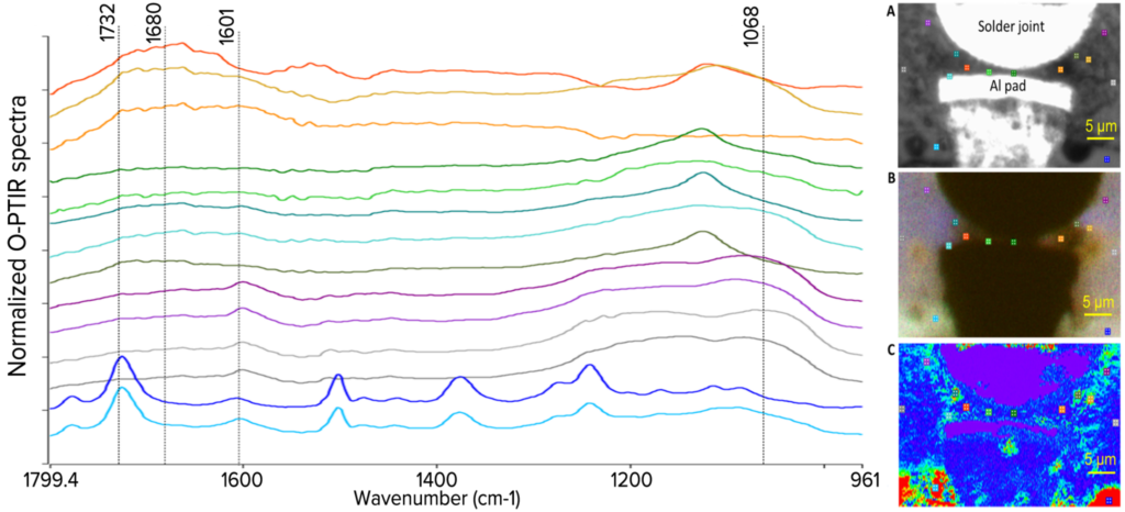
Figure 12 illustrates a newfound application of fluorescence imaging for identifying the dark ROI surrounding a solder joint which prevented it from making a good bond to an aluminum pad. The brightfield (BF) image seen in figure 12(a) allows users to locate the metallic surfaces from the underfill but chemical variation could not be discerned within the nearby organic matter. When the same ROI is separately illuminated with 497nm, 578nm and 628nm excitation lines, as shown in figure 12(b), relative FL intensities over the ROI could be rapidly recorded.
The overlaid FL image in figure 12(b) provides chemical contrast between the areas of the ROI, thus immediately providing locations for collecting O-PTIR spectra. These locations where not discernable in the BF image alone, as seen in figure 12(a). We can clearly see the underfill has drastically different chemistry than the contamination near the gap. The intensities of the changes are remarkable, suggesting location targets for acquiring O-PTIR spectra.
The utility of the FL images can be correlated with an O-PTIR image at 1732cm-1, shown in figure 12(c). The broad absorption around 1680cm-1 along with the warm colored markers are consistent with carboxylates; and the heightened absorption baseline arises from disordered carbon (Lo, 2021). Further away in the purple zone of figure 12 (b), the gray markers represent normal spectra consistent with the silica-enriched epoxy underfill. The purple spectra adjacent to the solder joint are within the slightly dimmer area than the bulk underfill on the FL image, which correlate well with the O-PTIR image for stronger IR absorption due to the presence of carbon. Finally, the brightest FL region comes from the polyimide solder resist, which is confirmed by those high-quality O-PTIR spectra consistent with polyimide (blue).
Once again, the multimodal mIRage-LS O-PTIR instrument with co-located FL can be equipped to work with dark and colored contamination at well-below visible laser damage thresholds, typically less than 0.1 mW. High spectral signal-to-noise could be readily achieved with ultra-sensitive avalanche photodiode (APD) detector.
Conclusion
O-PTIR on the mIRage and mIRage-LS platforms is a novel technique that overcomes the many of the limitations of conventional FTIR microscopy and spectroscopy, including its submicron IR spatial chemical resolution, enabling the broader use of IR for critical failure analysis related applications. O-PTIR also works in reflection mode with no scattering artifacts requiring zero or virtually zero sample preparation enabling faster time to data compared to traditional IR.
The use of APD detection with O-PTIR overcomes a major limitation of existing Raman spectroscopy techniques with colored and dark samples which would typically burn or produce low SNR data. O-PTIR collected with an APD detector with probe beam powers in the microwatt regime allow spectral to be collected at submicron resolution that would otherwise be impossible to collect.
O-PTIR also combines with Raman spectroscopy to provide simultaneous Raman and IR imaging and spectroscopy at the same measurement location, at the same time with the resolution. The combination provides complimentary and confirmatory results, while significantly improving time to data. Unknowns ID in FA is further enhanced when coupled with simultaneous IR and Raman spectral searching for more accurate identification.
- Semiconductor
- July 23, 2026
- Pharmaceuticals

- June 25, 2026
- Life Science | Microplastics

- May 28, 2026
- Products & Techniques

- April 30, 2026
- Life Science | Microplastics

- April 1, 2026
- Life Science | Microplastics

- March 19, 2026
Need more information?
Discover how O-PTIR technology can elevate your research or help solve your toughest challenges. Our team are happy to assist and answer your questions.